
Page 205 - Analog and Digital Filter Design
P. 205
202 Analog and Digital Filter Design
1
Remember that, at resonance, Fo =- so the inductor required to tune
2Km'
1
the highpass capacitor becomes LBS = , and the capacitor required
4~' Fo2CHp
1
to tune the highpass inductor becomes CBS =
47t'F0' LHp
For the bandstop filter tuned to 320 kHz, the frequency translating factor is
4n'Fo' = 4.04259 x 10". Using this information the bandstop circuit component
values are given in Table 7.1.
Highpzss Bandstop
Component Highpass Value Component Bandstop Value
L1 66.31 x C, 3.73045 x
C? 33.157 x L2 7.46045 x
L3 66.31 x Cj 3.73045 x
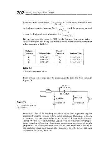
Putting these components into the circuit gives the bandstop filter shown in
Figure 7.4.
I
C2=33.157uF
Source -
L1=66.31 uH L3=66.31uH
R=l
-
Denormalization of the bandstop model for higher load impedance requires
component values to be scaled to have higher impedance. This is done in exactly
the same way that lowpass or highpass filters are scaled. Inductor values increase
in proportion to the load impedance. Capacitor values reduce inversely propor-
tional to the load. Capacitor values reduce because their impedance is inversely
proportional to their capacitance value. As the load impedance increases, all
the reactance values must increase their impedance in order to have the same
response as the prototype model.