
Page 206 - Analog and Digital Filter Design
P. 206
Bandstop Filters 20
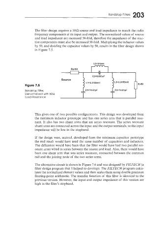
The filter design requires a 50Q source and load impedance to match the radio
frequency components at its input and output. The normalized values of source
and load impedance are increased 50-fold, therefore the impedance of the reac-
tive components must also be increased 50-fold. Multiplying the inductor values
by 50. and dividing the capacitor values by 50, results in the filter design shown
in Figure 7.5.
L2=373nH
L1=3.3155mH
Figure 7.5 R=50
Bandstop Filter,
Denormatized with 50 i2
toad Resistance
This gives one of two possible configurations. This design was developed from
the minimum inductor prototype and has one series arm that is parallel reso-
nant. It also has two shunt arms that are series resonant. The series resonant
shunt arms are connected across the input and the output terminals, so the input
impedance will be low in the stopband.
If the design were, instead, developed from the minimum capacitor prototype
the end result would have used the same number of capacitors and inductors.
The difference would have been that the filter would have had two parallel res-
onant arms wired in series between the source and Ioad. Also, there would have
been one shunt arm that was series resonant, connected between the common
rail and the joining node of the two series arms.
The alternative circuit is shown in Figure 7.6 and was designed by FILTECH (a
filter design program that I helped to develop). The FILTECH program caicu-
iates the normalized element values and then scales them using double precision
floating-point arithmetic. The transfer function of this filter is identical to the
previous version. However, the input and output impedance of this version are
high in the filter’s stopband.