
Page 211 - Analog and Digital Filter Design
P. 211
208 Analog and Digital Filter Design
L, = = 3.81493093 x
C2(P + 1)
but L/, = PLLl = 3.814930128 x lo-’
1 1
C, = - 262.128012 and C, = - 262.1279437
=
=
Lh L‘l
These component values must then be normalized. Multiply inductor values by
R and divide them by 2nF,. Divide capacitor values by 27rF”R. The value of L,,
then becomes 1.89738nH. Notice that only the value of C, from the highpass
prototype is required in these equations, in addition to P. In the equations that
will be given later, to convert the lowpass prototype directly into a bandstop
design, the value of L2 in the lowpass prototype will be used.
Now you may be wondering what to do with the shunt inductors in the high-
pass prototype. These are connected onto either side of the parallel tuned circuit
in my example. The answer is exactly the same as with all-pole filters; resonate
each shunt inductor with a series tuned capacitor at the stopband center fre-
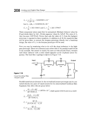
quency. The final filter topology is shown in Figure 7.10.
Ca Cb
Input II II output
-
R1
La Lb
Ll L3
R2
Figure 7.10
Cauer Bandstop Filter, == c1 == c3
1 Rad/S Cutoff
Parallel tuned circuit elements in the normalized lowpass prototype can be con-
verted directly into pairs of tuned circuits for the denormalized bandstop filter.
Equations that allow this are given below:
(Fc. - FL ) . RX
L,, = = 1.89738 X which agrees with the previous result.
(P + 1mF” FL