
Page 207 - Analog and Digital Filter Design
P. 207
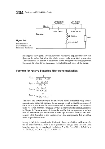
204 Analog and Digital Filter Design


                                                      L1=186.5nH      L3=186.5nH
                                            Rs=50


                                                     Cl=1.326uF        C3=1.326uF
                                    Source
                                                                                      R=50
                 Figure 7.6
                 Bandstop Filter.
                 Denormalized with
                 504 Load Resistance


                       Having gone through this laborious process, readers will be pleased to know that
                       there are formulae that  allow the whole process to be completed in one step.
                       These formulae are similar to those used in the bandpass filter design process.
                       Care must be taken to use the correct formulae for each stage of the design.


                 Formula for  Passive Bandstop Filter Denormalization


                       The series and shunt subscripts indicate which circuit element is being consid-
                       ered. A series subscript indicates the series arm (which is parallel resonant). A
                       shunt subscript indicates the shunt arm (which is series resonant). In the equa-
                       tions, the factor Xis the normalized lowpass element value taken from the tables
                       in Chapter 2. The same value of Xmust be used for both components in a single
                       branch. Remember that each branch in the all-pole lowpass filter has one com-
                       ponent, while branches in the bandstop have two components that are either
                       series or parallel resonant.

                       It may be helpful to redesign the third-order Butterworth filter to illustrate the
                       use  of  these  formulae.  Since it  is  a  symmetrical design,  only  the first  three
                       branches need  to be  calculated. As  before R  = 50, F,, = (320 + 1.2)  kHz  =
                       321.2kHz, FL=(320-  1.2) kHz= 318.8kHz.