Page 219 - Analog and Digital Filter Design
P. 219
2 1 6 Analog and Digital Filter Design


                                               R3            R3
                              These become,  R1= - and R2 =        for the bandstop filter.
                                                2          ~  4Q2  -2


                  Denormalization of  Bandstop Design Using MFBP Section

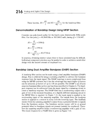
                        Consider one pole found earlier for the fourth-order Butterworth 50Hz notch
                        filter. For this polef,  = 48.58493Hz or 305.26812rad/s, having Q = 5.361447.


                                   R3
                              R1= - = 2795 Q
                                   2
                              R2=--   R3   - 49.47158 Q
                                   4Q2 -2
                        In practice, obtaining resistor values close to those calculated may be difficult.
                        Individual component selection may be needed in order to achieve a notch filter
                        design with the desired amount of  stopband loss.


                  Bandstop Using Dual Amplifier Bandpass (DABP) Section

                        A bandstop filter section can be made using a dual amplifier bandpass (DABP)
                        design. This is achieved by using a summing amplifier to subtract the bandpass
                        response from the input signal. The DABP topology is more complicated than
                        using the MFBP structure, but it has the advantage that much higher Q factors
                        can be achieved; Q factors of up to 150 are possible. The DABP is an all-pole
                        response bandpass ater section and has been described in Chapter 6. The band-
                        pass response can be subtracted from the input signal by a summing circuit to
                        create a bandstop response. The DABP filter has a noninverting output with a
                        gain of  two at the resonant frequency, so a slightly different summing circuit to
                        the MFBP filter is required. In Figure 7.14, the input signal is applied to the
                        noninverting input of  the summing amplifier. The output from the bandpass
                        section is applied to a resistor in series with the inverting input. The feedback
                        resistor from the summing amplifier’s output forms a potential divider to signals
                        from  the  bandpass  section. The  bandpass  section  output  will  be  at  ground
                        potential when no bandpass signals are present (outside the stopband). There-
                        fore the summing amplifier forms a noninverting amplifier with a gain of two.
                        The circuit diagram for a DABP filter is given in Figure 7.14.

