
Page 220 - Analog and Digital Filter Design
P. 220
Bandstop Filters 21
ut
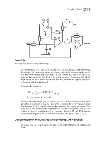
Figure 7.14
Bandstop Filter Section Using DABP Design
The capacitance of C1 and C2 should be equal but may have any arbitrary value.
In practice, the capacitors’ values are chosen so that the resistors’ values are all
in a reasonable range, typically from lk!2 to 100kQ. The limits are up to the
designer. but remember that R3 and R4 load the output of op-amps A 1 and A2.
High values of R1 will introduce noise, and may degrade the signals, because it
is in series with the signal path.
Consider the equations:
R1=- (2 and R2 = R3 =- 1
2K. fRC> 2K. fRC
In other words R1 = Q. R2.
If the section’s Q is high, say 75. then RI will be 75 times R2 and R3. The value
of Cshould be chosen so that the value of R1 is close to the lower resistance limit.
The value of R2 will then be close to the recommended upper resistance limit.
This circuit has independent adjustment of resonant frequency and Q. The
resistor R1 is used to adjust the (2 at resonance. Resistor R? and R3 determine
the resonant frequency. At the resonant frequency. the gain is fixed at GR = 2.
Denormalization of Bandstop Design Using DABP Section
Consider one pole found earlier for the fourth-order Butterworth 50Hz notch
filter.