
Page 362 - Analog and Digital Filter Design
P. 362
359
Introduction to Digital Filters
w,
h(0) = -
n
where n = 0.
To produce the desired frequency response we must have an impulse response
that produces an output before the impulse arrives! This is impossible. The solu-
tion is to delay the signal, so that some signal processing takes place before the
peak of the impulse response arrives at the output. The longer the delay: the
closer we get to the ideal frequency response. Limiting the period during which
signal processing takes place is known as truncation. This can lead to rounding
of the passband edge and ripples in the stopband.
A 1 radts lowpass filter can now be designed using discrete logic. First build a
chain of delay elements. usually these are D-type flip-flops clocked by the master
clock. Each delay element is 10 bits wide. From the output of each stage take
the digitized signal and multiply it by the value of the impulse response that
corresponds to that moment in time. An example will help explain this further.
Suppose we have 21 delay elements. Delay elements 1 to 10 produce the nega-
tive time outputs, delay element 11 corresponds with the zero time output, and
delay elements 12 to 21 are the positive time outputs.
The output from delay element 1 will be multiplied by the value of the
impulse response at -20 seconds, to give product one. In Figure 15.2 the impulse
response value is approximately 0.01453 at -20 seconds, where t = -2000
hundredths of a second. The next delay element output will be multiplied
by the impulse response at -18 seconds, to give product two. Further delay
element outputs are multiplied by the impulse response at -16, -14, -12. -10.
-8. -6, -4, -2, 0, 2, 4, 6, 8, 10, 12, 14, 16, 18, and 20 seconds. to give products
3 to 21. All these products must now be added together, to form the filter’s
output signal.
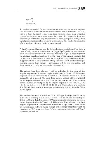
The hardware we need is as follows: 21 x 10 D-type flip-flops; and 21 rnulri-
pliers and a summing circuit with 21 inputs. This list omitted the analog-to-
digital (MD) and digital-to-analog (D/A) conkerters at the input and output. A
circuit diagram is given in Figure 15.3. This type of filter is known as a finite
impulse response (FIR) filter because, if there are 21 taps. after 21 clock pulses
an impulse signal will have passed through and no longer affect the output. In
this diagram, “D” represents a delay, “x” represents a multiplication, and ”Sum”
represents an addition.