
Page 363 - Analog and Digital Filter Design
P. 363
360 Analog and Digital Filter Design
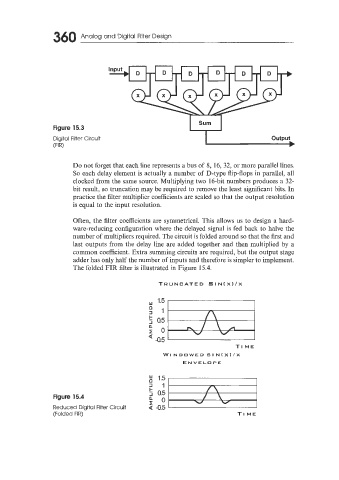
Figure 15.3
Digital Filter Circuit
(FIR)
Do not forget that each line represents a bus of 8, 16, 32, or more parallel lines.
So each delay element is actually a number of D-type flip-flops in parallel, all
clocked from the same source. Multiplying two 16-bit numbers produces a 32-
bit result, so truncation may be required to remove the least significant bits. In
practice the filter multiplier coefficients are scaled so that the output resolution
is equal to the input resolution.
Often, the filter coefficients are symmetrical. This allows us to design a hard-
ware-reducing configuration where the delayed signal is fed back to halve the
number of multipliers required. The circuit is folded around so that the first and
last outputs from the delay line are added together and then multiplied by a
common coefficient. Extra summing circuits are required, but the output stage
adder has only half the number of inputs and therefore is simpler to implement.
The folded FIR filter is illustrated in Figure 15.4.
TRUNCATED SIN(X)/X
1.5
I-
1 0.5
U
E O
a 4.5
TI ME
WINDOWED SI N(X)/X
ENVELOPE
1 1
F I\
Figure 15.4 Ij 0.5 /\
a 0 v
z