
Page 209 - Analytical Electrochemistry 2d Ed - Jospeh Wang
P. 209
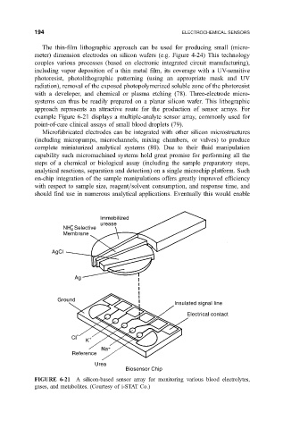
194                                           ELECTROCHEMICAL SENSORS

              The thin-®lm lithographic approach can be used for producing small (micro-
            meter) dimension electrodes on silicon wafers (e.g. Figure 4-24) This technology
            couples various processes (based on electronic integrated circuit manufacturing),
            including vapor deposition of a thin metal ®lm, its coverage with a UV-sensitive
            photoresist, photolithographic patterning (using an appropriate mask and UV
            radiation), removal of the exposed photopolymerized soluble zone of the photoresist
            with a developer, and chemical or plasma etching (78). Three-electrode micro-
            systems can thus be readily prepared on a planar silicon wafer. This lithographic
            approach represents an attractive route for the production of sensor arrays. For
            example Figure 6-21 displays a multiple-analyte sensor array, commonly used for
            point-of-care clinical assays of small blood droplets (79).
              Microfabricated electrodes can be integrated with other silicon microstructures
            (including micropumps, microchannels, mixing chambers, or valves) to produce
            complete miniaturized analytical systems (80). Due to their ¯uid manipulation
            capability such micromachined systems hold great promise for performing all the
            steps of a chemical or biological assay (including the sample preparatory steps,
            analytical reactions, separation and detection) on a single microchip platform. Such
            on-chip integration of the sample manipulations offers greatly improved ef®ciency
            with respect to sample size, reagent=solvent consumption, and response time, and
            should ®nd use in numerous analytical applications. Eventually this would enable


            FIGURE 6-21  A silicon-based sensor array for monitoring various blood electrolytes,
            gases, and metabolites. (Courtesy of i-STAT Co.)