
Page 224 - Complete Wireless Design
P. 224
Oscillator Design
Oscillator Design 223
sent a typical crystal for an oscillator using the manufacturer’s above motion-
al specifications of L ,C ,R , and C .
m m m p
Note that if a crystal’s holder or its package is changed, as might be required
when redesigning for a smaller oscillator, this will have an effect on the above
motional properties of the crystal, and a new simulation must be performed
with these latest values to assure proper operation.
A word on open-loop simulation using a Spice simulator. We can obtain accu-
rate design results when simulating low-frequency oscillators with Spice,
especially when we must employ a low-frequency transistor for which there
are no S-parameters available. Bode plotters, as well as the AC analysis tool
in Spice simulators, may not give accurate loop gain measurements unless we
attach a basic Spice frequency source (set to 1 Hz) through a 50-ohm resistor
to the oscillator’s “input” (the LC resonator at the node between C and L of
1 1
an LC oscillator). However, the resonant frequency at maximum gain as indi-
cated in the Bode plotter and the AC analysis tool window will vary slightly
from the other, as will the 0 degree phase-crossing frequency.
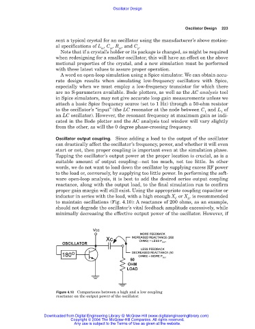
Oscillator output coupling. Since adding a load to the output of the oscillator
can drastically affect the oscillator’s frequency, power, and whether it will even
start or not, then proper coupling is important even at the simulation phase.
Tapping the oscillator’s output power at the proper location is crucial, as is a
suitable amount of output coupling—not too much, not too little. In other
words, we do not want to load down the oscillator by supplying excess RF power
to the load or, conversely, by supplying too little power. In performing the soft-
ware open-loop analysis, it is best to add the desired series output coupling
reactance, along with the output load, to the final simulation run to confirm
proper gain margin will still exist. Using the appropriate coupling capacitor or
inductor in series with the load, with a high enough X or X , is recommended
C L
to maintain oscillations (Fig. 4.10): A reactance of 200 ohms, as an example,
should not degrade the oscillator’s vital feedback amplitude excessively, while
minimally decreasing the effective output power of the oscillator. However, if
Figure 4.10 Comparisons between a high and a low coupling
reactance on the output power of the oscillator.
Downloaded from Digital Engineering Library @ McGraw-Hill (www.digitalengineeringlibrary.com)
Copyright © 2004 The McGraw-Hill Companies. All rights reserved.
Any use is subject to the Terms of Use as given at the website.