
Page 234 - Complete Wireless Design
P. 234
Oscillator Design
Oscillator Design 233
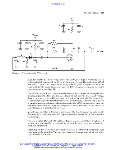
Figure 4.18 A complete bipolar VCO circuit.
R and R are the BJT’s bias components, and the C ’s are bypass capacitors chosen
b c B
to decouple all frequencies from 60 Hz all the way to f , and beyond, with an X of
OUT C
less than 1 ohm. This necessitates using various types of capacitors, such as
electrolytic for the audio frequencies and two different value ceramic (or porcelain)
capacitors for low and high RF.
The varactor bias voltage, chosen from the varactor’s data sheet for the capacitance
desired, employs the RFC and the R to block RF but pass the DC control voltage.
V
Since a varactor is reversed biased, very little leakage current will flow through R ,
V
so the voltage dropped across this resistor will be quite small. The varactor is chosen
to supply an appropriate range of capacitances for the VCO’s tuning range, since the
only component that will vary the frequency of oscillation will be the varactor’s
capacitance, which is controlled by V .
CNTRL
Q will have an f that is 5 times or more above the f frequency so as to closely
1 t OUT
maintain the common emitter’s 180 degree phase shift across the oscillator’s entire
tuning range.
The C ’s are placed to block DC, but to easily pass f . C will have a high X (50
C OUT COUP C
to 200), and can readily be replaced by an equally high reactance inductor for
harmonic suppression.
Depending on the frequencies of oscillation chosen, a varactor of sufficiently high
value may not be available. This can be overcome by increasing L, which will allow
D to be decreased in value.
1
Downloaded from Digital Engineering Library @ McGraw-Hill (www.digitalengineeringlibrary.com)
Copyright © 2004 The McGraw-Hill Companies. All rights reserved.
Any use is subject to the Terms of Use as given at the website.