
Page 232 - Complete Wireless Design
P. 232
Oscillator Design
Oscillator Design 231
I
D
V V 1
GS P I
DSS
f. RFC equals 1000 ohms.
g. C 1 ohm (X )
C C
h. L RFC
2
2. Confirm that the JFET device will safely dissipate the power of:
P I V
D D
3. To design the resonant LC network:
258 1 1
L C C
1 2 f D1 480 f 2 48 f
4. Couple the output of the oscillator to its 50-ohm load through a 200- to 600-
ohm reactance (C ), which can be either inductive or capacitive.
COUP
5. Simulate and optimize as explained in Sec. 4.1, “Oscillator Simulation.”
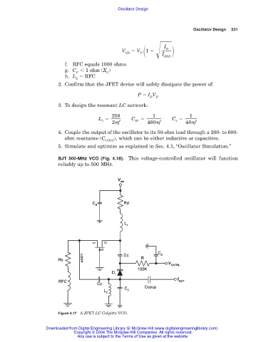
BJT 500-MHz VCO (Fig. 4.18). This voltage-controlled oscillator will function
reliably up to 500 MHz.
Figure 4.17 A JFET LC Colpitts VCO.
Downloaded from Digital Engineering Library @ McGraw-Hill (www.digitalengineeringlibrary.com)
Copyright © 2004 The McGraw-Hill Companies. All rights reserved.
Any use is subject to the Terms of Use as given at the website.