
Page 230 - Complete Wireless Design
P. 230
Oscillator Design
Oscillator Design 229
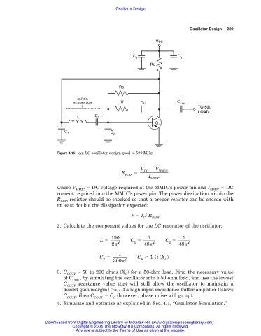
Figure 4.15 An LC oscillator design good to 500 MHz.
V V
MMIC
CC
R
BIAS I
MMIC
where V DC voltage required at the MMIC’s power pin and I DC
MMIC MMIC
current required into the MMIC’s power pin. The power dissipation within the
R BIAS resistor should be checked so that a proper resistor can be chosen with
at least double the dissipation expected:
P I 2 R
C BIAS
2. Calculate the component values for the LC resonator of the oscillator:
190 1 1
L C C
2 f 1 48 f 2 48 f
1
C C 1 (X )
3 300 f B C
3. C ≈ 50 to 200 ohms (X ) for a 50-ohm load. Find the necessary value
COUP C
of C by simulating the oscillator into a 50-ohm load, and use the lowest
COUP
C reactance value that will still allow the oscillator to maintain a
COUP
decent gain margin ( 5). If a high input impedance buffer amplifier follows
C , then C C (however, phase noise will go up).
COUP COUP C
4. Simulate and optimize as explained in Sec. 4.1, “Oscillator Simulation.”
Downloaded from Digital Engineering Library @ McGraw-Hill (www.digitalengineeringlibrary.com)
Copyright © 2004 The McGraw-Hill Companies. All rights reserved.
Any use is subject to the Terms of Use as given at the website.