Page 265 - Complete Wireless Design
P. 265
Frequency Synthesizer Design


            264  Chapter Five

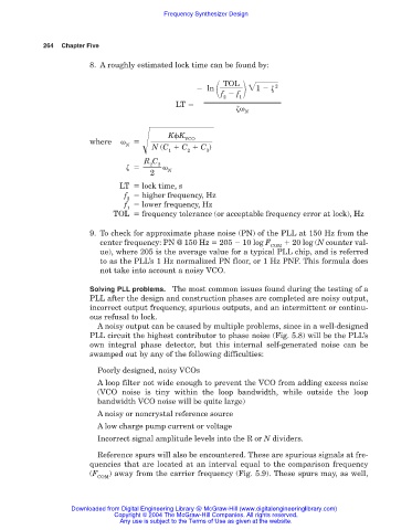
                        8. A roughly estimated lock time can be found by:


                                                           TOL
                                                      ln     1          2
                                                          f   f
                                                               1
                                                           2
                                              LT

                                                                N
                                             K K
                                                 VCO
                        where
                                  N
                                         )
                                        N (C   C   C
                                                 2
                                             1
                                                      3
                                      R C
                                          2
                                        2

                                        2   N
                                LT   lock time, s
                                 f   higher frequency, Hz
                                  2
                                 f   lower frequency, Hz
                                  1
                              TOL   frequency tolerance (or acceptable frequency error at lock), Hz
                        9. To check for approximate phase noise (PN) of the PLL at 150 Hz from the
                           center frequency: PN @ 150 Hz   205   10 log F    20 log (N counter val-
                                                                       COM
                           ue), where 205 is the average value for a typical PLL chip, and is referred
                           to as the PLL’s 1 Hz normalized PN floor, or 1 Hz PNF. This formula does
                           not take into account a noisy VCO.
                        Solving PLL problems. The most common issues found during the testing of a
                        PLL after the design and construction phases are completed are noisy output,
                        incorrect output frequency, spurious outputs, and an intermittent or continu-
                        ous refusal to lock.
                          A noisy output can be caused by multiple problems, since in a well-designed
                        PLL circuit the highest contributor to phase noise (Fig. 5.8) will be the PLL’s
                        own integral phase detector, but this internal self-generated noise can be
                        swamped out by any of the following difficulties:
                          Poorly designed, noisy VCOs
                          A loop filter not wide enough to prevent the VCO from adding excess noise
                          (VCO noise is tiny within the loop bandwidth, while outside the loop
                          bandwidth VCO noise will be quite large)
                          A noisy or noncrystal reference source
                          A low charge pump current or voltage
                          Incorrect signal amplitude levels into the R or N dividers.

                          Reference spurs will also be encountered. These are spurious signals at fre-
                        quencies that are located at an interval equal to the comparison frequency
                        (F   ) away from the carrier frequency (Fig. 5.9). These spurs may, as well,
                          COM


                   Downloaded from Digital Engineering Library @ McGraw-Hill (www.digitalengineeringlibrary.com)
                               Copyright © 2004 The McGraw-Hill Companies. All rights reserved.
                                Any use is subject to the Terms of Use as given at the website.

