
Page 262 - Complete Wireless Design
P. 262
Frequency Synthesizer Design
Frequency Synthesizer Design 261
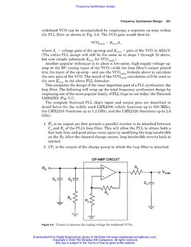
wideband VCO can be accomplished by employing a separate op-amp within
the PLL filter as shown in Fig. 5.6. The VCO gain would then be:
VCO K A
GAIN VCO v
where A voltage gain of the op-amp and K gain of the VCO in MHz/V.
v VCO
(The entire PLL design will still be the same as in steps 1 through 10 above,
but now simply substitute K for VCO .)
VCO GAIN
Another popular technique is to place a low-noise, high-supply-voltage op-
amp at the DC tuning input of the VCO—with the loop filter’s output placed
into the input of the op-amp—and use the VCO formula above to calculate
GAIN
the new gain of the VCO. The result of the VCO calculation will be used as
GAIN
the new K in the above PLL formulas.
VCO
This completes the design of the most important part of a PLL synthesizer, the
loop filter. The following will wrap up the total frequency synthesizer design by
employing one of the most popular family of PLL chips in use today: the National
LMX23XX (Fig. 5.7).
The complete National PLL chip’s input and output pins are described in
detail below for the widely used LMX2306 (which functions up to 550 MHz),
the LMX2316 (functions up to 1.2 GHz), and the LMX2326 (functions up to 2.8
GHz):
1. Fl is an output pin that permits a parallel resistor to be attached between
o
C and R of the PLL’s loop filter. This will allow the PLL to obtain both a
2 2
fast lock time and good phase noise specs by modifying the loop bandwidth
on the fly. After the channel change occurs, loop bandwidth reverts back to
normal.
2. CP is the output of the charge pump to which the loop filter is attached.
o
Figure 5.6 Circuit to increase the tuning voltage for wideband VCOs.
Downloaded from Digital Engineering Library @ McGraw-Hill (www.digitalengineeringlibrary.com)
Copyright © 2004 The McGraw-Hill Companies. All rights reserved.
Any use is subject to the Terms of Use as given at the website.