
Page 43 - Complete Wireless Design
P. 43
Wireless Essentials
42 Chapter One
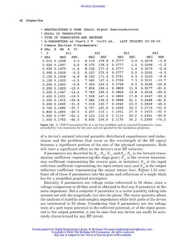
Figure 1.52 A *.S2P S-parameter file at a set bias condition and at assorted frequencies. Lines
preceded by ! are comments for the user and are ignored by the simulation programs.
of a device’s natural internal parasitic distributed capacitances and induc-
tances and the problems that occur as the wavelength of the RF signal
becomes a significant portion of the size of the physical components. Both
will have a significant effect on the device’s true RF behavior.
S parameters are described by S , S , S , and S . S is the forward trans-
21 12 11 22 21
mission coefficient (representing the stage gain); S is the reverse transmis-
12
sion coefficient (representing the reverse gain, or isolation); S is the input
11
reflection coefficient (representing the input return loss); and S is the output
22
reflection coefficient (representing the output return loss). Figure 1.53 com-
bines all of these S parameters into the gains and reflections of a single black
box for a simplified graphical description.
Basically, S parameters are voltage ratios referenced to 50 ohms, since a
voltage comparison is all that need be obtained to find any S parameter at the
same impedance. But a complete S parameter is a vector quantity, taking into
account not only the magnitude, but also the phase. The vector quantity allows
the analysis of stability and complex impedances while both ports of the device
are terminated in 50 ohms. Considering that S parameters are the voltage
ratio of a port input potential to the reflected potential, or of the input poten-
tial to the output potential, it can be seen that any device can easily be accu-
rately characterized for any RF circuit.
Downloaded from Digital Engineering Library @ McGraw-Hill (www.digitalengineeringlibrary.com)
Copyright © 2004 The McGraw-Hill Companies. All rights reserved.
Any use is subject to the Terms of Use as given at the website.