
Page 213 -
P. 213
5.5 / KEY TERMS, REVIEW QUESTIONS, AND PROBLEMS 181
5.9 What is a parity bit?
5.10 How is the syndrome for the Hamming code interpreted?
5.11 How does SDRAM differ from ordinary DRAM?
Problems
5.1 Suggest reasons why RAMs traditionally have been organized as only 1 bit per chip
whereas ROMs are usually organized with multiple bits per chip.
5.2 Consider a dynamic RAM that must be given a refresh cycle 64 times per ms. Each re-
fresh operation requires 150 ns; a memory cycle requires 250 ns. What percentage of
the memory’s total operating time must be given to refreshes?
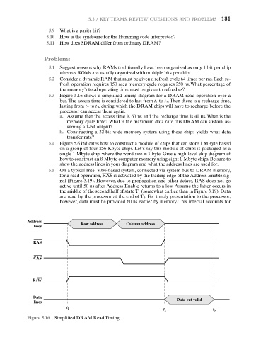
5.3 Figure 5.16 shows a simplified timing diagram for a DRAM read operation over a
bus. The access time is considered to last from t 1 to t 2 . Then there is a recharge time,
lasting from t 2 to t 3 , during which the DRAM chips will have to recharge before the
processor can access them again.
a. Assume that the access time is 60 ns and the recharge time is 40 ns. What is the
memory cycle time? What is the maximum data rate this DRAM can sustain, as-
suming a 1-bit output?
b. Constructing a 32-bit wide memory system using these chips yields what data
transfer rate?
5.4 Figure 5.6 indicates how to construct a module of chips that can store 1 MByte based
on a group of four 256-Kbyte chips. Let’s say this module of chips is packaged as a
single 1-Mbyte chip, where the word size is 1 byte. Give a high-level chip diagram of
how to construct an 8-Mbyte computer memory using eight 1-Mbyte chips. Be sure to
show the address lines in your diagram and what the address lines are used for.
5.5 On a typical Intel 8086-based system, connected via system bus to DRAM memory,
for a read operation, RAS is activated by the trailing edge of the Address Enable sig-
nal (Figure 3.19). However, due to propagation and other delays, RAS does not go
active until 50 ns after Address Enable returns to a low. Assume the latter occurs in
the middle of the second half of state T 1 (somewhat earlier than in Figure 3.19). Data
are read by the processor at the end of T 3 . For timely presentation to the processor,
however, data must be provided 60 ns earlier by memory. This interval accounts for
Address
lines Row address Column address
RAS
CAS
R/W
Data
lines Data out valid
t 1
t 2 t 3
Figure 5.16 Simplified DRAM Read Timing