
Page 208 -
P. 208
176 CHAPTER 5 / INTERNAL MEMORY
Table 5.4 SDRAM Pin Assignments
A0 to A13 Address inputs
CLK Clock input
CKE Clock enable
CS Chip select
RAS Row address strobe
CAS Column address strobe
WE Write enable
DQ0 to DQ7 Data input/output
DQM Data mask
The SDRAM employs a burst mode to eliminate the address setup time and row and
column line precharge time after the first access. In burst mode, a series of data bits
can be clocked out rapidly after the first bit has been accessed. This mode is useful
when all the bits to be accessed are in sequence and in the same row of the array as
the initial access. In addition, the SDRAM has a multiple-bank internal architecture
that improves opportunities for on-chip parallelism.
The mode register and associated control logic is another key feature differen-
tiating SDRAMs from conventional DRAMs. It provides a mechanism to customize
the SDRAM to suit specific system needs. The mode register specifies the burst
length, which is the number of separate units of data synchronously fed onto the
bus. The register also allows the programmer to adjust the latency between receipt
of a read request and the beginning of data transfer.
The SDRAM performs best when it is transferring large blocks of data seri-
ally, such as for applications like word processing, spreadsheets, and multimedia.
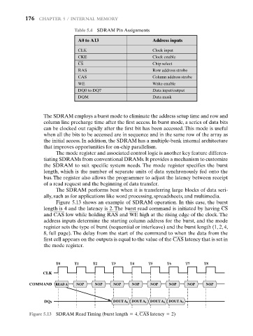
Figure 5.13 shows an example of SDRAM operation. In this case, the burst
length is 4 and the latency is 2. The burst read command is initiated by having CS
and CAS low while holding RAS and WE high at the rising edge of the clock. The
address inputs determine the starting column address for the burst, and the mode
register sets the type of burst (sequential or interleave) and the burst length (1, 2, 4,
8, full page). The delay from the start of the command to when the data from the
first cell appears on the outputs is equal to the value of the CAS latency that is set in
the mode register.
T0 T1 T2 T3 T4 T5 T6 T7 T8
CLK
COMMAND READ A NOP NOP NOP NOP NOP NOP NOP NOP
DQs DOUT A 0 DOUT A 1 DOUT A 2 DOUT A 3
Figure 5.13 SDRAM Read Timing (burst length = 4, CAS latency = 2)