
Page 205 -
P. 205
174 CHAPTER 5 / INTERNAL MEMORY
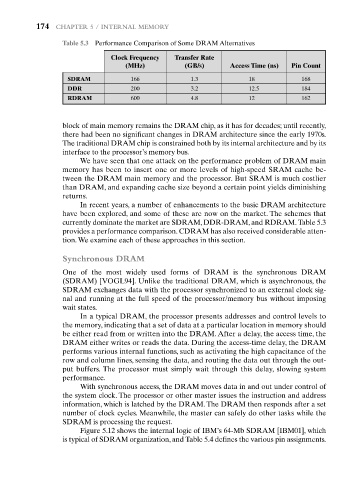
Table 5.3 Performance Comparison of Some DRAM Alternatives
Clock Frequency Transfer Rate
(MHz) (GB/s) Access Time (ns) Pin Count
SDRAM 166 1.3 18 168
DDR 200 3.2 12.5 184
RDRAM 600 4.8 12 162
block of main memory remains the DRAM chip, as it has for decades; until recently,
there had been no significant changes in DRAM architecture since the early 1970s.
The traditional DRAM chip is constrained both by its internal architecture and by its
interface to the processor’s memory bus.
We have seen that one attack on the performance problem of DRAM main
memory has been to insert one or more levels of high-speed SRAM cache be-
tween the DRAM main memory and the processor. But SRAM is much costlier
than DRAM, and expanding cache size beyond a certain point yields diminishing
returns.
In recent years, a number of enhancements to the basic DRAM architecture
have been explored, and some of these are now on the market. The schemes that
currently dominate the market are SDRAM, DDR-DRAM, and RDRAM. Table 5.3
provides a performance comparison. CDRAM has also received considerable atten-
tion.We examine each of these approaches in this section.
Synchronous DRAM
One of the most widely used forms of DRAM is the synchronous DRAM
(SDRAM) [VOGL94]. Unlike the traditional DRAM, which is asynchronous, the
SDRAM exchanges data with the processor synchronized to an external clock sig-
nal and running at the full speed of the processor/memory bus without imposing
wait states.
In a typical DRAM, the processor presents addresses and control levels to
the memory, indicating that a set of data at a particular location in memory should
be either read from or written into the DRAM. After a delay, the access time, the
DRAM either writes or reads the data. During the access-time delay, the DRAM
performs various internal functions, such as activating the high capacitance of the
row and column lines, sensing the data, and routing the data out through the out-
put buffers. The processor must simply wait through this delay, slowing system
performance.
With synchronous access, the DRAM moves data in and out under control of
the system clock. The processor or other master issues the instruction and address
information, which is latched by the DRAM. The DRAM then responds after a set
number of clock cycles. Meanwhile, the master can safely do other tasks while the
SDRAM is processing the request.
Figure 5.12 shows the internal logic of IBM’s 64-Mb SDRAM [IBM01], which
is typical of SDRAM organization, and Table 5.4 defines the various pin assignments.