
Page 209 -
P. 209
5.3 / ADVANCED DRAM ORGANIZATION 177
There is now an enhanced version of SDRAM, known as double data rate
SDRAM (DDR-SDRAM) that overcomes the once-per-cycle limitation. DDR-
SDRAM can send data to the processor twice per clock cycle.
Rambus DRAM
RDRAM, developed by Rambus [FARM92, CRIS97], has been adopted by Intel for
its Pentium and Itanium processors. It has become the main competitor to SDRAM.
RDRAM chips are vertical packages, with all pins on one side. The chip exchanges
data with the processor over 28 wires no more than 12 centimeters long.The bus can
address up to 320 RDRAM chips and is rated at 1.6 GBps.
The special RDRAM bus delivers address and control information using an
asynchronous block-oriented protocol.After an initial 480 ns access time, this pro-
duces the 1.6 GBps data rate. What makes this speed possible is the bus itself,
which defines impedances, clocking, and signals very precisely. Rather than being
controlled by the explicit RAS, CAS, R/W, and CE signals used in conventional
DRAMs, an RDRAM gets a memory request over the high-speed bus. This re-
quest contains the desired address, the type of operation, and the number of bytes
in the operation.
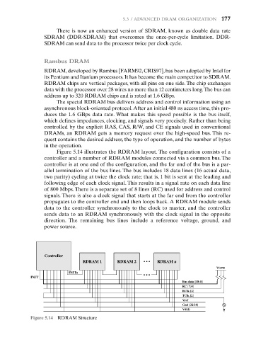
Figure 5.14 illustrates the RDRAM layout. The configuration consists of a
controller and a number of RDRAM modules connected via a common bus. The
controller is at one end of the configuration, and the far end of the bus is a par-
allel termination of the bus lines. The bus includes 18 data lines (16 actual data,
two parity) cycling at twice the clock rate; that is, 1 bit is sent at the leading and
following edge of each clock signal. This results in a signal rate on each data line
of 800 Mbps. There is a separate set of 8 lines (RC) used for address and control
signals. There is also a clock signal that starts at the far end from the controller
propagates to the controller end and then loops back. A RDRAM module sends
data to the controller synchronously to the clock to master, and the controller
sends data to an RDRAM synchronously with the clock signal in the opposite
direction. The remaining bus lines include a reference voltage, ground, and
power source.
Controller
RDRAM 1 RDRAM 2 • • • RDRAM n
Vterm
INITo
• • •
INIT
Bus data [18:0]
RC [7:0]
RClk [2]
TClk [2]
Vref
Gnd (32/18)
Vd(4)
Figure 5.14 RDRAM Structure