
Page 210 -
P. 210
178 CHAPTER 5 / INTERNAL MEMORY
DDR SDRAM
SDRAM is limited by the fact that it can only send data to the processor once per
bus clock cycle.A new version of SDRAM, referred to as double-data-rate SDRAM
can send data twice per clock cycle, once on the rising edge of the clock pulse and
once on the falling edge.
DDR DRAM was developed by the JEDEC Solid State Technology Associa-
tion, the Electronic Industries Alliance’s semiconductor-engineering-standardization
body. Numerous companies make DDR chips, which are widely used in desktop
computers and servers.
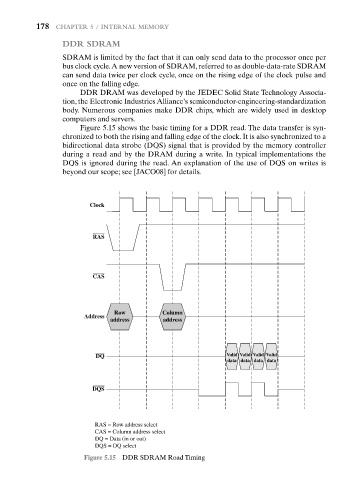
Figure 5.15 shows the basic timing for a DDR read. The data transfer is syn-
chronized to both the rising and falling edge of the clock. It is also synchronized to a
bidirectional data strobe (DQS) signal that is provided by the memory controller
during a read and by the DRAM during a write. In typical implementations the
DQS is ignored during the read. An explanation of the use of DQS on writes is
beyond our scope; see [JACO08] for details.
Clock
RAS
CAS
Row Column
Address
address address
DQ Valid Valid Valid Valid
data data data data
DQS
RAS = Row address select
CAS = Column address select
DQ = Data (in or out)
DQS = DQ select
Figure 5.15 DDR SDRAM Road Timing