Page 214 -
P. 214

182  CHAPTER 5 / INTERNAL MEMORY

                        propagation delays along the data paths (from memory to processor) and processor
                        data hold time requirements.Assume a clocking rate of 10 MHz.
                        a. How fast (access time) should the DRAMs be if no wait states are to be inserted?
                        b. How many wait states do we have to insert per memory read operation if the ac-
                           cess time of the DRAMs is 150 ns?
                    5.6  The memory of a particular microcomputer is built from 64K *  1 DRAMs. Accord-
                        ing to the data sheet, the cell array of the DRAM is organized into 256 rows. Each
                        row must be refreshed at least once every 4 ms. Suppose we refresh the memory on a
                        strictly periodic basis.
                        a. What is the time period between successive refresh requests?
                        b. How long a refresh address counter do we need?


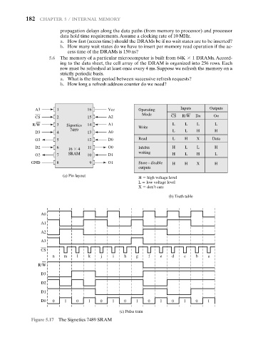
               A3      1           16     Vcc         Operating       Inputs     Outputs
                                                       Mode        CS  R/W  Dn     On
               CS      2           15     A2
             R/W       3   Signetics  14  A1                       L    L   L      L
                                                      Write
                            7489                                   L    L   H      H
               D3      4           13     A0
               O3      5           12     D0          Read         L    H   X     Data
               D2      6   16   4  11     O0          Inhibit      H    L   L      H
               O2      7   SRAM    10     D1          writing      H    L   H      L
             GND       8           9      O1          Store - disable  H  H  X     H
                                                      outputs
                                                      H   high voltage level
                                                      L   low voltage level
                                                      X   don’t care

                                                                  (b) Truth table


                 A0
                 A1
                 A2
                 A3

                 CS
                     n    m    l   k    j   i    h   g    f   e    d    c   b    a
                R/W
                 D3
                 D2

                 D1
                 D0  0    1   0    1   0    1    0   1    0   1    0   1    0    1
                                               (c) Pulse train
             Figure 5.17 The Signetics 7489 SRAM
   209   210   211   212   213   214   215   216   217   218   219