
Page 341 - DSP Integrated Circuits
P. 341
326 Chapter 7 DSP System Design
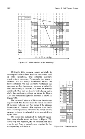
Figure 7.55 ASAP schedule of the inner loop
Obviously, this memory access schedule is
unacceptable since there are four concurrent read
or write operations. This schedule therefore
requires four memories. Fortunately, the memory
accesses are not evenly distributed within the
folded schedule. We can therefore reschedule the
processes so that the memory accesses are distrib-
uted more evenly in time and still meet the memory
constraint. This can be done by introducing extra
slack time (shimming delay), as shown in Figure
7.57. The corresponding folded schedule is shown in
Figure 7.58.
The increased latency will increase the storage
requirement. The Address must be stored for either
15 memory cycles or only four cycles if the address
is recomputed. However, this requires extra hard-
ware. The WP processes (WP) must be stored for two
memory cycles or be scheduled to be computed two
cycles later.
The inputs and outputs of the butterfly opera-
tions must also be stored as shown in Figure 7.59.
Thus, only four registers, one for each complex data
word to and from a butterfly, are required in the
corresponding architecture. Figure 7.56 Folded schedule