
Page 340 - DSP Integrated Circuits
P. 340
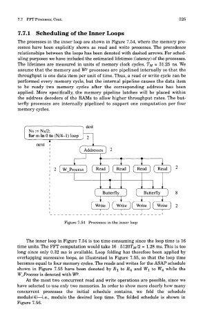
7.7 FFT Processor, Cont.                                              325

        7.7.1 Scheduling of the Inner Loops

        The processes in the inner loop are shown in Figure 7.54, where the memory pro-
        cesses have been explicitly shown as read and write processes. The precedence
        relationships between the loops has been denoted with dashed arrows. For sched-
        uling purposes we have included the estimated lifetimes (latency) of the processes.
        The lifetimes are measured in units of memory clock cycles, TM = 31.25 ns. We
        assume that the memory and WP processes are pipelined internally so that the
        throughput is one data item per unit of time. Thus, a read or write cycle can be
        performed every memory cycle, but the internal pipeline causes the data item
        to be ready two memory cycles after the corresponding address has been
        applied. More specifically, the memory pipeline latches will be placed within
        the address decoders of the RAMs to allow higher throughput rates. The but-
        terfly processes are internally pipelined to support one computation per four
        memory cycles.


                            Figure 7.54 Processes in the inner loop


            The inner loop in Figure 7.54 is too time consuming since the loop time is 16
        time units. The FFT computation would take 16 • 5120T M/2 = 1.28 ms. This is too
        long since only 0.32 ms is available. Loop folding has therefore been applied by
        overlapping successive loops, as illustrated in Figure 7.55, so that the loop time
        becomes equal to four memory cycles. The reads and writes for the ASAP schedule
        shown in Figure 7.55 have been denoted by RI to R^ and Wi to W^ while the
        W_Process is denoted with WP.
            At the most two concurrent read and write operations are possible, since we
        have selected to use only two memories. In order to show more clearly how many
        concurrent processes the initial schedule contains, we fold the schedule
        modulo(4)—i.e., modulo the desired loop time. The folded schedule is shown in
        Figure 7.56.