
Page 47 - DSP Integrated Circuits
P. 47
32 Chapter 2 VLSI Circuit Technologies
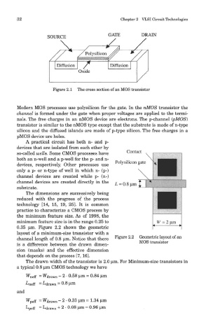
Figure 2.1 The cross section of an MOS transistor
Modern MOS processes use polysilicon for the gate. In the nMOS transistor the
channel is formed under the gate when proper voltages are applied to the termi-
nals. The free charges in an nMOS device are electrons. The p-channel (pMOS)
transistor is similar to the nMOS type except that the substrate is made of n-type
silicon and the diffused islands are made of p-type silicon. The free charges in a
pMOS device are holes.
A practical circuit has both n- and p-
devices that are isolated from each other by
so-called wells. Some CMOS processes have
both an n-well and a p-well for the p- and n-
devices, respectively. Other processes use
only a p- or n-type of well in which n- (p-)
channel devices are created while p- (n-)
channel devices are created directly in the
substrate.
The dimensions are successively being
reduced with the progress of the process
technology [14, 15, 19, 25]. It is common
practice to characterize a CMOS process by
the minimum feature size. As of 1998, the
minimum feature size is in the range 0.25 to
0.35 |j,m. Figure 2.2 shows the geometric
layout of a minimum-size transistor with a
channel length of 0.8 um. Notice that there Figure 2.2 Geometric layout of an
MOS transistor
is a difference between the drawn dimen-
sion (masks) and the effective dimension
that depends on the process [7,16].
The drawn width of the transistor is 2.0 (im. For Minimum-size transistors in
a typical 0.8 fim CMOS technology we have