
Page 52 - DSP Integrated Circuits
P. 52
2.3 MOS Logic 37
Dynamic logic circuits are based on the temporary storage of information as
charges in stray and gate capacitances. The charges must therefore be periodically
restored. This is done by transferring the charges between different storing capac-
itances and at the same time performing the logic functions. An external control
signal (i.e. a clock) is required to control the transfer of information in dynamic cir-
cuits. Advantages of dynamic logic circuits are higher clock frequencies, often
lower power consumption, and smaller chip area. The main drawback is that the
noise margin is only about Vji Hence, special care has to be taken to reduce the
noise.
In MOS logic circuits the output node of a logic circuit is connected via a con-
ducting transistor network to a logic signal source, except during switching
between the two states. This source can be either VDD, Gnd, or an input signal. In
the case of VDD or Gnd the output signal level is restored. To transfer the correct
logic value sufficiently fast to the next stage, the depth of the network must be
small.
2.3.1 nMOS Logic
Generally, a logic function is implemented using a circuit that implements the so-
called switching function. We will use the following notation:
F(A, B, ...) = logic function to be implemented as a circuit
S(A, B, ...) = switching function implemented as a transistor network
Networks that can be successively described by serial and/or parallel connec-
tions between switches and subnetworks can be analyzed by a form of Boolean
0
aigeora —switcnmg aigeora;.
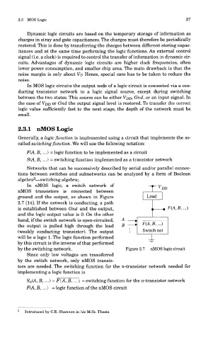
In nMOS logic, a switch network of
nMOS transistors is connected between
ground and the output, as shown in Figure
2.7 [14]. If the network is conducting, a path
is established between Gnd and the output,
and the logic output value is 0. On the other
hand, if the switch network is open-circuited,
the output is pulled high through the load
(weakly conducting transistor). The output
will be a logic 1. The logic function performed
by this circuit is the inverse of that performed
by the switching network. Figure 2.7 nMOS logic circuit
Since only low voltages are transferred
by the switch network, only nMOS transis-
tors are needed. The switching function for the n-transistor network needed for
implementing a logic function is
S n(A, B, ...) = F(A, B, ...) = switching function for the n-transistor network
F(A, B, ...) = logic function of the nMOS circuit
3
- Introduced bv C.E. Shannon in his M.Sc. Thesis.