
Page 48 - DSP Integrated Circuits
P. 48
2.2 MOS Transistors 33
The MOS transistor is a four-terminal
device: source, gate, drain, and substrate
(well). The source of a transistor is denned so
that the charges in the channel move from
the source toward the drain. For example, for
an n-channel transistor the moving charges
are electrons. Here, the source is the termi-
nal that has the lowest potential. The termi-
nal with the highest potential is the source
for a p-channel transistor since the moving
charges are holes.
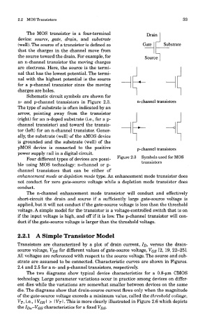
Schematic circuit symbols are shown for
n- and p-channel transistors in Figure 2.3.
The type of substrate is often indicated by an
arrow, pointing away from the transistor
(right) for an n-doped substrate (i.e., for a p-
channel transistor) and toward the transis-
tor (left) for an n-channel transistor. Gener-
ally, the substrate (well) of the nMOS device
is grounded and the substrate (well) of the
pMOS device is connected to the positive
power supply rail in a digital circuit.
Four different types of devices are possi- Figure 2.3 Symbols used for MOS
ble using MOS technology: n-channel or p- transistors
channel transistors that can be either of
enhancement mode or depletion mode type. An enhancement mode transistor does
not conduct for zero gate-source voltage while a depletion mode transistor does
conduct.
The n-channel enhancement mode transistor will conduct and effectively
short-circuit the drain and source if a sufficiently large gate-source voltage is
applied, but it will not conduct if the gate-source voltage is less than the threshold
voltage. A simple model for the transistor is a voltage-controlled switch that is on
if the input voltage is high, and off if it is low. The p-channel transistor will con-
duct if the gate-source voltage is larger than the threshold voltage.
2.2.1 A Simple Transistor Model
Transistors are characterized by a plot of drain current, ID, versus the drain-
source voltage, YDS for different values of gate-source voltage, VQS [2, 19, 22-25].
All voltages are referenced with respect to the source voltage. The source and sub-
strate are assumed to be connected. Characteristic curves are shown in Figures.
2.4 and 2.5 for a n- and p-channel transistors, respectively.
The two diagrams show typical device characteristics for a 0.8-um CMOS
technology. Large parameter variations occur in practice among devices on differ-
ent dies while the variations are somewhat smaller between devices on the same
die. The diagrams show that drain-source current flows only when the magnitude
of the gate-source voltage exceeds a minimum value, called the threshold voltage,
VT, i.e., I VQS I > I Vy I. This is more clearly illustrated in Figure 2.6 which depicts
the IDTI—VGS characteristics for a fixed Vrjg-