
Page 50 - DSP Integrated Circuits
P. 50
2.2 MOS Transistors 35
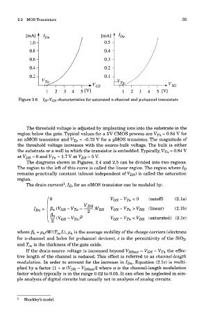
Figure 2.6 ID~VGS characteristics for saturated n-channel and p-channel transistors
The threshold voltage is adjusted by implanting ions into the substrate in the
region below the gate. Typical values for a 5V CMOS process are VT H ~ 0-84 V for
an nMOS transistor and VT P ~ -0.73 V for a pMOS transistor. The magnitude of
the threshold voltage increases with the source-bulk voltage. The bulk is either
the substrate or a well in which the transistor is embedded. Typically, VT H ~ 0.84 V
at V DS = 0 and V Tn - 1.7 V at V DS = 5 V.
The diagrams shown in Figures. 2.4 and 2.5 can be divided into two regions.
The region to the left of this curve is called the linear region. The region where /D
remains practically constant (almost independent of V#s) is called the saturation
region.
1
The drain current , ID, for an nMOS transistor can be modeled by:
where (3 n = n neW/(T oxL), ]ii n is the average mobility of the charge carriers (electrons
for n-channel and holes for p-channel devices), e is the permittivity of the SiO2,
and T ox is the thickness of the gate oxide.
=
If the drain-source voltage is increased beyond Vpssat VGS ~ ^Tn the effec-
tive length of the channel is reduced. This effect is referred to as channel-length
modulation. In order to account for the increase in ID H, Equation (2.1c) is multi-
plied by a factor [1 + a (Vps - Vassal where a is the channel-length modulation
factor which typically is in the range 0.02 to 0.05. It can often be neglected in sim-
ple analysis of digital circuits but usually not in analysis of analog circuits.
1
- Shockley's model.