
Page 54 - DSP Integrated Circuits
P. 54
2.3 MOS Logic 39
to get a sufficiently low output voltage. It is therefore preferable to use NOR gates
instead of NAND gates, since the n-devices, in the former case, are connected in
parallel.
The main drawbacks with nMOS logic circuits are the static power dissipation
and the fact that a logic 0 at the output is obtained as a ratio between two imped-
ances. The ratio is critical to the function of the gate and requires careful design.
The load can be implemented using either a resistor or an nMOS transistor. The
nMOS transistor can be of the enhancement type, operating in either the satu-
rated or nonsaturated region, or of the depletion type. The best overall perfor-
mance for nMOS circuits is obtained by using depletion mode load transistors, but
then some extra steps in the fabrication process are needed.
2.3.2 CMOS Logic Circuits
4
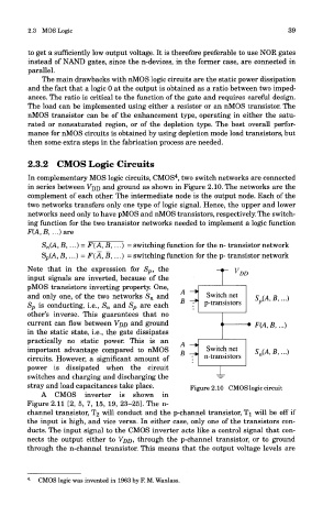
In complementary MOS logic circuits, CMOS , two switch networks are connected
an
in series between VQD d ground as shown in Figure 2.10. The networks are the
complement of each other. The intermediate node is the output node. Each of the
two networks transfers only one type of logic signal. Hence, the upper and lower
networks need only to have pMOS and nMOS transistors, respectively. The switch-
ing function for the two transistor networks needed to implement a logic function
F(A,B, ...)are
S n(A, B,...) = F(A, B, ...) = switching function for the n- transistor network
S p(A, B, ...) = F(A, B, ...) = switching function for the p- transistor network
Note that in the expression for S p, the
input signals are inverted, because of the
pMOS transistors inverting property. One,
and only one, of the two networks S n and
S p is conducting, i.e., S n and S p are each
other's inverse. This guarantees that no
current can flow between VDD and ground
in the static state, i.e., the gate dissipates
practically no static power. This is an
important advantage compared to nMOS
circuits. However, a significant amount of
power is dissipated when the circuit
switches and charging and discharging the
stray and load capacitances take place. Figure 2.10 CMOS logic circuit
A CMOS inverter is shown in
Figure 2.11 [2, 5, 7, 15, 19, 23-25]. The n-
channel transistor, T£ will conduct and the p-channel transistor, TI will be off if
the input is high, and vice versa. In either case, only one of the transistors con-
ducts. The input signal to the CMOS inverter acts like a control signal that con-
nects the output either to VDD, through the p-channel transistor, or to ground
through the n-channel transistor. This means that the output voltage levels are
4
- CMOS logic was invented in 1963 by F. M. Wanlass.