
Page 58 - DSP Integrated Circuits
P. 58
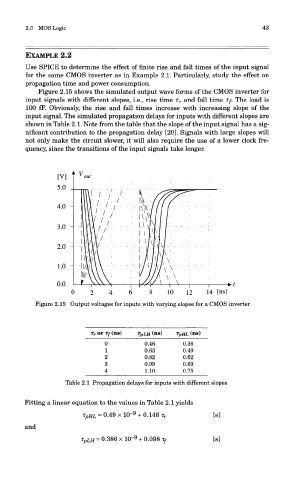
2.3 MOS Logic                                                         43


        EXAMPLE 2.2
        Use SPICE to determine the effect of finite rise and fall times of the input signal
        for the same CMOS inverter as in Example 2.1. Particularly, study the effect on
        propagation time and power consumption.
            Figure 2.15 shows the simulated output wave forms of the CMOS inverter for
        input signals with different slopes, i.e., rise time r r and fall time if. The load is
        100 fF. Obviously, the rise and fall times increase with increasing slope of the
        input signal. The simulated propagation delays for inputs with different slopes are
        shown in Table 2.1. Note from the table that the slope of the input signal has a sig-
        nificant contribution to the propagation delay [20]. Signals with large slopes will
        not only make the circuit slower, it will also require the use of a lower clock fre-
        quency, since the transitions of the input signals take longer.


           Figure 2.15 Output voltages for inputs with varying slopes for a CMOS inverter


                           T r or Tf (ns)  r pLH (ns)  T pHL (ns)
                               0           0.46        0.36
                                1           0.63       0.49
                               2           0.82       0.62
                               3           0.99        0.69
                               4           1.10       0.75
                    Table 2.1 Propagation delays for inputs with different slopes

        Fitting a linear equation to the values in Table 2.1 yields


        and