
Page 61 - DSP Integrated Circuits
P. 61
46 Chapter 2 VLSI Circuit Technologies
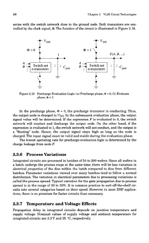
series with the switch network close to the ground node. Both transistors are con-
trolled by the clock signal, O. The function of the circuit is illustrated in Figure 2.18.
Figure 2.18 Precharge-Evaluation Logic: (a) Precharge phase, <I> = 0, (b) Evaluate
phase, O= l
In the precharge phase, <D = 0, the precharge transistor is conducting. Thus,
n
the output node is charged to VDD- I the subsequent evaluation phase, the output
signal value will be determined. If the expression F is evaluated to 0, the switch
network will conduct and discharge the output node. On the other hand, if the
expression is evaluated to 1, the switch network will not conduct, and the output is
a "floating" node. Hence, the output signal stays high as long as the node is
charged. The input signal must be valid and stable during the evaluation phase.
The lowest operating rate for precharge-evaluation logic is determined by the
charge leakage from node F.
2.3.6 Process Variations
Integrated circuits are processed in batches of 50 to 200 wafers. Since all wafers in
a batch undergo the process steps at the same time, there will be less variation in
electrical properties of the dice within the batch compared to dice from different
batches. Parameter variations viewed over many batches tend to follow a normal
distribution. The variation in electrical parameters due to processing variations is
called the process spread. Typical variation for the gate propagation due to process
spread is in the range of 30 to 50%. It is common practice to sort off-the-shelf cir-
cuits into several categories based on their speed. However, in most DSP applica-
tions, there is no premium for faster circuits than necessary.
2.3.7 Temperature and Voltage Effects
Propagation delay in integrated circuits depends on junction temperature and
supply voltage. Nominal values of supply voltage and ambient temperature for
integrated circuits are 3.3 V and 25 °C, respectively.