
Page 63 - DSP Integrated Circuits
P. 63
48 Chapter 2 VLSI Circuit Technologies
The contribution from excess temperature, TA, process spread, and reduced volt-
age is
Thus, the circuit should be designed with nominal parameter values to run with a
clock frequency that exceeds the required frequency by 50%. Typical worst-case
factors are 1.7 for commercial circuits (70°C, 3.135 V) and 2.2 for military circuits
(125 °C, 3.0 V) where the two temperatures indicate the worst-case ambient tem-
perature.
2.4 VLSI PROCESS TECHNOLOGIES
There are several types of CMOS processes, for example, bulk CMOS and CMOS-
SOI (silicon-on-insulator) [12, 13]. In bulk CMOS, the transistor function takes
place at the surface and within the substrate while in CMOS-SOI it takes place in
material placed on top of an insulator. In the early bulk CMOS technologies, the
gate was formed of metal—metal gate CMOS—while in modern CMOS technolo-
gies the gate is formed of polysilicon—silicon gate CMOS. Thus, the term MOS
itself is no longer appropriate.
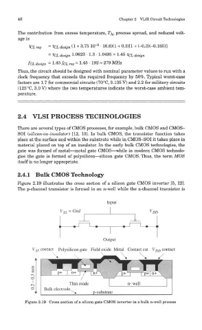
2.4.1 Bulk CMOS Technology
Figure 2.19 illustrates the cross section of a silicon gate CMOS inverter [5, 121.
The p-channel transistor is formed in an n-well while the n-channel transistor is
Figure 2.19 Cross section of a silicon gate CMOS inverter in a bulk n-well process