
Page 68 - DSP Integrated Circuits
P. 68
2.5 Trends in CMOS Technologies 53
thermal conductivity and low hole mobility compared to silicon devices. This
means that GaAs is not suitable for complementary circuit styles.
2.5 TRENDS IN CMOS TECHNOLOGIES
The future isn't what it used to be.
—Arthur C. Clarke
The current trend in process technology is toward dense and high-speed CMOS
circuits while at the same time the economical chip area increases. The reduction
of the dimensions of MOS devices improves both the circuit performance and the
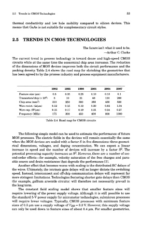
packing density. Table 2.4 shows the road map for shrinking the geometries that
has been agreed to by the process industry and process equipment manufacturers.
1992 1995 1998 2001 2004 2007
Feature size (urn) 0.5 0.35 0.25 0.18 0.13 0.1
6
Transistors/chip (x 10 ) 5 10 21 46 110 260
2
Chip area (mm ) 210 250 300 360 430 520
Wire resist. (Q/jim) 0.12 0.15 0.19 0.29 0.82 1.34
Wire cap. (fF/pm) 0.15 0.17 0.19 0.21 0.24 0.27
Frequency (MHz) 175 300 450 600 800 1000
Table 2.4 Road map for CMOS circuits
The following simple model can be used to estimate the performance of future
MOS processes. The electric fields in the devices will remain essentially the same
when the MOS devices are scaled with a factor S in five dimensions: three geomet-
rical dimensions, voltages, and doping concentration. We can expect a linear
2
increase in speed and the number of devices will increase by a factor S . The
3
potential processing capacity increases as S . However, there are a number of sec-
ond-order effects—for example, velocity saturation of the free charges and para-
sitic source and drain resistances that degrade the performance [3].
Another effect that becomes worse with scaling is the distributed RC delays of
the wires. Ultimately, the intrinsic gate delays will no longer dictate the switching
speed. Instead, interconnect and off-chip communication delays will represent far
more stringent limitations. Technologies featuring shorter gate delays than CMOS
(for example, gallium arsenide circuits) will therefore not necessarily prevail in
the long term.
The constant field scaling model shows that smaller feature sizes will
require lowering of the power supply voltage. Although it is still possible to use
the standard 5-V power supply for micrometer technologies, submicron processes
will require lower voltages. Typically, CMOS processes with minimum feature
sizes of 0.5 |j,m use a supply voltage of VDD = 3.3 V. However, this supply voltage
can only be used down to feature sizes of about 0.4 um. For smaller geometries,