
Page 67 - DSP Integrated Circuits
P. 67
52 Chapter 2 VLSI Circuit Technologies
with the complex (large) circuits and low power dissipation that is characteristic of
CMOS technology. However, only a small fraction of the devices on a VLSI chip can
be bipolar, because of the high power dissipation [1, 8, 17]. The bipolar devices
(ECL gates) should therefore be used only in the most time-critical paths of the
circuit and for driving large capacitive loads. In practice, BiCMOS circuits have a
speed advantage of a factor of about 2 over pure CMOS circuits. BiCMOS technol-
ogies are also suitable for mixed analog-digital circuits, since bipolar transistors
have higher transconductance and generate less noise.
The use of BiCMOS will prolong the lifetime of CMOS technologies and allow
them to compete with pure bipolar and GaAs technologies in high-speed applica-
tion. The fabrication process is more complex for BiCMOS compared to CMOS.
2.4.6 GaAs-Based Technologies
Gallium arsenide VLSI circuits are competing with silicon-based technologies as a
viable VLSI technology [4, 6, 9, 11, 18, 26]. The potential switching speed of this
technology is higher than for state-of-the-art ECL (emitter-coupled logic) while the
power consumption is lower. GaAs circuits are also better suited in environments
with ionizing radiation and they can operate at a wider temperature range than
silicon devices. The high switching speed is due to the high electron mobility and
the small parasitic capacitances that are due to the insulating substrate. The
small parasitic capacitances contribute to low power consumption.
There are three major types of GaAs devices: (1) MESFET (metal-semiconduc-
tor field-effect transistor), (2) HEMT (high electron mobility transistor), also called
MODFET (modulation doped FET), and (3) HBT (Heterojunction Bipolar Transis-
tor) [3]. GaAs is basically a NOR gate technology. Buffered Direct-Coupled FET
logic; (BDCFL) is the dominant logic family.
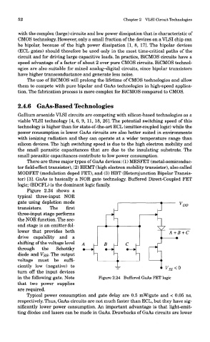
Figure 2.24 shows a
typical three-input NOR
gate using depletion mode
transistors. The first
three-input stage performs
the NOR function. The sec-
ond stage is an emitter-fol-
lower that provides both
drive capability and a
shifting of the voltage level
through the Schottky
diode and V$s- The output
voltage must be suffi-
ciently low (negative) to
turn off the input devices
in the following gate. Note Figure 2.24 Buffered GaAs FET logic
that two power supplies
are required.
Typical power consumption and gate delay are 0.5 mW/gate and < 0.05 ns,
respectively. Thus, GaAs circuits are not much faster than ECL, but they have sig-
nificantly lower power consumption. An important advantage is that light-emit-
ting diodes and lasers can be made in GaAs. Drawbacks of GaAs circuits are lower