
Page 64 - DSP Integrated Circuits
P. 64
2.4 VLSI Process Technologies 49
formed directly in the substrate, which is of p-type. Since hole mobility is lower
than for electrons, the p-channel device is usually made wider than the n-channel
device to obtain a symmetric switching behavior. The input capacitance to an
inverter is about three times the gate capacitance for the n-channel device.
Latch-up due to parasitic tyristors is a problem that may appear in CMOS cir-
cuits. Latch-up causes excessive power supply current to flow and may even destroy
the circuit. There is no way to turn the tyristor off except for disconnecting the
power supply. An early technique to avoid latch-up was to use so-called guard bands
of heavy doped material between n- and p-devices while modern processes, as the
one illustrated in Figure 2.19, use field oxide to isolate the different types of devices.
2.4.2 Silicon-on-Insulation (SOI) Technology
Silicon-on-insulation technology is a serious contender for the fabrication of future
integrated circuits. Compatibility with ordinary CMOS circuit styles, excellent
device scalability, better device and circuit performance, low power consumption,
high working temperatures (200 to 300°C), radiation-hardness, and potentially
lower cost are the main reasons. An early type of SOI was SOS (silicon-on-sapphire)
[12]. This material was costly and had poor quality. It was used primarily in mili-
tary and aerospace applications because of the excellent radiation-hardness.
SIMOX (separation by implantation of oxygen) is today the most widely used SOI
technology. It is produced by an implantation of a high dose of oxygen ions into a
silicon wafer, followed by an annealing at very high temperature to finally form a
well-defined buried silicon dioxide layer beneath a single-crystal silicon top layer
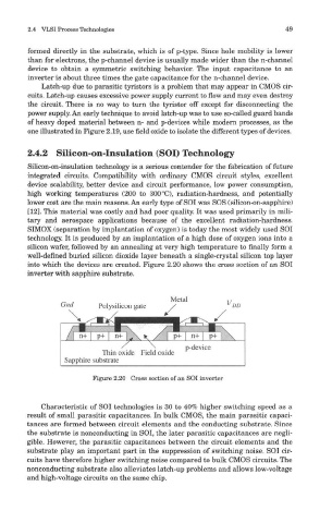
into which the devices are created. Figure 2.20 shows the cross section of an SOI
inverter with sapphire substrate.
Figure 2.20 Cross section of an SOI inverter
Characteristic of SOI technologies is 30 to 40% higher switching speed as a
result of small parasitic capacitances. In bulk CMOS, the main parasitic capaci-
tances are formed between circuit elements and the conducting substrate. Since
the substrate is nonconducting in SOI, the later parasitic capacitances are negli-
gible. However, the parasitic capacitances between the circuit elements and the
substrate play an important part in the suppression of switching noise. SOI cir-
cuits have therefore higher switching noise compared to bulk CMOS circuits. The
nonconducting substrate also alleviates latch-up problems and allows low-voltage
and high-voltage circuits on the same chip.