
Page 59 - DSP Integrated Circuits
P. 59
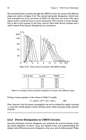
44                                          Chapter 2 VLSI Circuit Technologies


        The simulated drain currents through the CMOS inverter for inputs with different
        slopes are shown in Figure 2.16. The current and power dissipation, which have
        been averaged over 15 ns, are shown in Table 2.2. Also here, the slope of the input
        signal causes a small increase in power dissipation. The increase in power dissipa-
        tion is due to the increase in the time interval when both devices conduct and a
        small current flows directly through the two transistors.


                     Figure 2.16 Drain currents for inputs with different slopes


                         T r orT/>(ns)  WMA)           P(»tW)
                             0            32.0          160.0
                             1            31.9          159.5
                             2            33.3          166.5
                             3            35.1          175.5
                             4            37.2          186.0
             Table 2.2 Average current and power dissipation for inputs with different slopes


        Fitting a linear equation to the values in Table 2.2 yields
                                             6
                               P = 155.9 x 10-  + 6.8 x 10³ T r  [W]
        Note, however, that the power consumption can not be reduced by simply reducing
        r r, since this would require a faster driving source which consumes large amounts
        of power.


        2.3.4 Power Dissipation in CMOS Circuits
        Accurate estimates of power dissipation are necessary for several reasons: avoid-
        ing metal migration in power (Vp/)) and ground wires, and understanding the
        design trade-off between power dissipation, chip area, and switching speed. Today