
Page 56 - DSP Integrated Circuits
P. 56
2.3 MOS Logic 41
Speed and power dissipation of dig-
ital circuits can be estimated using a
simple model that neglects the short-
circuit current flowing during a transi-
tion. This assumption is reasonable if
the slope of the input signal is large.
Ideally, the input signal is a step func-
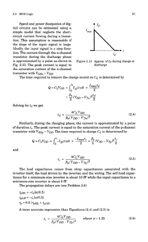
tion. The current through the n-channel
transistor during the discharge phase
is approximated by a pulse as shown in Figure 2.13 Approx. of ID during charge or
Fig. 2.13. The peak current is equal to discharge
the saturation current of the n-channel
transistor with VoSn ~ VDD-
The time required to remove the charge stored on CL is determined by
Solving for t& we get
Similarly, during the charging phase, the current is approximated by a pulse
of duration t c. The peak current is equal to the saturation current of the p-channel
=
transistor with VsGp VDD- The time required to charge CL is determined by
and
The load capacitance comes from stray capacitances associated with the
inverter itself, the load driven by the inverter, and the wiring. The self-load capac-
itance for a minimum-size inverter is about 10 fF while the input capacitance to a
minimum-size inverter is about 8 fF.
The propagation delays are (see Problem 2.6)
A more accurate expression than Equations (2.4) and (2.5) is