
Page 55 - DSP Integrated Circuits
P. 55
40 Chapter 2 VLSI Circuit Technologies
Figure 2.11 CMOS inverter
independent of the relative sizes of the p- and n-channel devices. CMOS logic is
therefore referred to as ratioless logic. This implies that CMOS circuits produce a
larger output voltage swing, resulting in a higher noise immunity than the corre-
sponding nMOS circuits. The p-transistor is often made wider than the corre-
sponding n-channel transistor to get symmetric switching times.
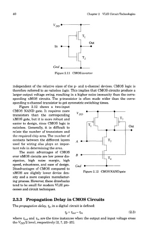
figure z.iz snows a two-input
CMOS NAND gate. It requires more
transistors than the corresponding
nMOS gate, but it is more robust and
easier to design, since CMOS logic is
ratioless. Generally, it is difficult to
relate the number of transistors and
the required chip area. The number of
contacts between the different layers
used for wiring also plays an impor-
tant role in determining the area.
The main advantages of CMOS
over nMOS circuits are low power dis-
sipation, high noise margin, high
speed, robustness, and ease of design.
Disadvantages of CMOS compared to
Figure 2.12 CMOS NAND gate
nMOS are slightly lower device den-
sity and a more complex manufactur-
ing process. However, these drawbacks
tend to be small for modern VLSI pro-
cesses and circuit techniques.
2.3.3 Propagation Delay in CMOS Circuits
The propagation delay, T p, in a digital circuit is defined:
where i out and T/ n are the time instances when the output and input voltage cross
the V DD/2 level, respectively [2, 7, 23-25].