
Page 60 - DSP Integrated Circuits
P. 60
2.3 MOS Logic 45
power consumption is one of the most important constraints in integrated circuit
design.
The current in a wire must not be too large because of electromigration [2,7].
2
Typically, a metal wire may not carry a current of more than ~ I mA/(|Lim) . A min-
5
imum-width metal 2 wire (width = 1.6 um and thickness of 1 um) that is used for
power and ground routing can therefore only support up to 1.6 mA/35 joA ~ 45 min-
imum-size CMOS inverters of the type used in Example 2.2. The lower layer
(metal 1) has typically a thickness of only 0.6 urn.
As mentioned before, CMOS circuits have negligible static power dissipation.
The leakage current is in the nanoampere range. Typically the power consumption
due to leakage is less than 1% of the total power consumption. If the slope of the
input signal is small or the transistor sizes are very large, as is the case in large
buffers, a power supply current flows when both the p- and n-transistors conduct.
However, for normal logic gates and input signals, the power consumption due to
this current is less than 10% of the total power consumption. Significant power is
dissipated when the output switches from one state to the other. The stray and
load capacitances are, during a complete switch cycle, charged and discharged
through the p-transistor and the n-transistor, respectively. Thus, the average
power supply current is
if the inverter is switched with the frequency/", and A Vis the output voltage swing.
The swing for CMOS circuits is typically VDD- The power dissipation associated
with the CMOS inverter is
With C L = 105 fF, V DD = 5 V, and /= 1/16 ns = 62.5 MHz, we get an average
power dissipation of 156.3 uW, which agrees well with the values in Table 2.2.
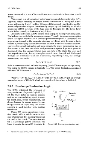
2.3.5 Precharge-Evaluation Logic
The 1990s witnessed the proposals of
many variations of dynamic logic [2, 5, 7,
23—25]. They differ in various aspects,
such as maximum clocking speed, transis-
tor count, area, power consumption, and
charge leakage in storage nodes. In pre-
charge-evaluation logic, only one switch
network is used together with clocking
transistors.
Figure 2.17 shows a precharge-evalua-
tion circuit with a switch network with
only n-transistors. Two clocking transistors
are used in this circuit. The upper transis-
tor is a precharge pMOS transistor. The
lower transistor is an nMOS transistor in Figure 2.17 Precharge-e valuation logic
5
- The second metal layer, on top of the first metal layer (metal 1), is called metal 2.