
Page 65 - DSP Integrated Circuits
P. 65
50 Chapter 2 VLSI Circuit Technologies
2.4.3 Bipolar Technologies—TTL
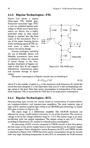
Figure 2.21 shows a typical
three-input TTL NAND gate.
Transistor-transistor logic (TTL)
is now an outdated bipolar tech-
nology in which one or more tran-
sistors are driven into a highly
saturated state so that excess
charge is injected into the base
region of the transistors. This is
one of the major limiting factors
of the switching speed of TTL cir-
cuits since it takes time to
remove the excess charge.
Various strategies, including
the use of Schottky diodes and
Schottky transistors, have been
introduced to reduce the amount
of excess charge in the base.
Another drawback of bipolar cir-
cuits is that they do not support Figure 2.21 TTL NAND gate
bidirectional transmission gates
and dynamic storage of signal
values.
The power consumption of bipolar circuits due to switching is
where N is the number of gates, f max is the maximum clock frequency for which the
circuit has been designed, C is the equivalent load, and AVis the corresponding volt-
age swing at the load. Note that power consumption is independent of the actual
clock frequency. TTL is unsuitable for VLSI due to its large power consumption.
2.4.4 Bipolar Technologies—ECL
Nonsaturating logic circuits are usually based on combinations of emitter-follow-
ers (common-collector) and common-base amplifiers. The most common type of
logic is ECL (emitter-coupled logic) which is an OR-NOR gate technology. A typical
ECL gate is shown in Figure 2.22.
The input stage is a differential amplifier. The OR-NOR functions are
obtained by using a multi-emitter transistor in one of the branches. The crossover
voltage is set by the voltage reference stage to -1.2 V. The output stage is an emit-
ter-follower with low output impedance. The output swing is only 0.8 V which,
according to Equation(2.12), results in reduced power consumption.
An advantage of ECL circuits compared to CMOS circuits is that they gener-
ate less noise on the power supply lines so that requirements on the power supply
are less stringent. Power dissipation versus frequency for ECL and CMOS circuits
is sketched in Figure 2.23. CMOS has lower power consumption except for circuits
with very high switching frequencies. In fact, ECL is unsuitable for VLSI because