
Page 57 - DSP Integrated Circuits
P. 57
42 Chapter 2 VLSI Circuit Technologies
EXAMPLE 2.1
Estimate the propagation delay for a CMOS inverter that is loaded with five iden-
tical inverters connected in parallel. The wiring corresponds to a load of about 5 fF.
Compare the result with a SPICE simulation. Use the following values:
The effective load is
Substituting into Equations (2.4) and (2.5) we get the charge and discharge times:
t c = 1.24 ns and tj = 0.61 ns. Now, the propagation delay is
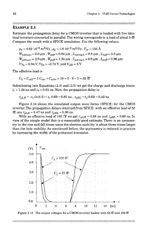
Figure 2.14 shows the simulated output wave forms (SPICE) for the CMOS
inverter. The propagation delays obtained from SPICE, with an effective load of 55
fF, are T PLH ~ 0-47 ns and T PHL ~ 0-36 ns.
With an effective load of 105 fF we get T: PLH ~ 0-88 ns and T: PHL ~ 0.68 ns. In
view of the simple model this is a reasonably good estimate. There is an asymme-
try in the rise and fall times since the electron mobility is about three times larger
than the hole mobility. As mentioned before, the asymmetry is reduced in practice
by increasing the width of the p-channel transistor.
Figure 2.14 The output voltages for a CMOS inverter loaded with 55 fF and 105 fF