
Page 53 - DSP Integrated Circuits
P. 53
38 Chapter 2 VLSI Circuit Technologies
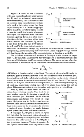
Figure 2.8 shows an nMOS inverter
with an n-channel depletion mode transis-
tor, TI and an n-channel enhancement
mode transistor T%. The inverter itself has
an intrinsic stray capacitance and is typi-
cally used to drive other gates that have
capacitive inputs. It is therefore appropri-
ate to model the inverter's typical load by
a capacitor which the inverter charges or
discharges. The depletion mode transistor
is called a pull-up device. It is often conve-
nient to model this transistor with a (non-
linear) resistor. The transistor, T%, acts as
a pull-down device. The pull-down transis-
tor will be off if the input to the inverter is
lower than the threshold voltage, \Tn- Therefore, the output of the inverter will be
charged to VDD by the conducting pull-up transistor. Only a negligible leakage current
will flow through the transistors. The power dissipation in this state is negligible.
The pull-down transistor will conduct if the input to the inverter is larger
than VT- In this state, a current will flow through both of the transistors and the
inverter will dissipate a significant amount of power. The output voltage, when the
output is low, is determined by the ratio of the effective drain-source resistances:
nMOS logic is therefore called ratioed logic. The output voltage should ideally be
zero for a perfect inverter. However, to be able to drive another inverter or gate,
the output has only to be sufficiently low, that is, less than the threshold voltage of
the following stage. For example, assume that VDD = 5 V and VT = 1V. This implies
that R\ » 4 R% and the effective load capacitance, CL, will discharge through R^
at least four times faster during the pull-down phase than during the pull-up
phase. This asymmetry of switching times is a major problem in ratioed logic.
Now, RI must be made small in order to
obtain fast switching circuits. This leads to an
even smaller value for R<z in order to satisfy the
ratio criterion just discussed. Small effective
drain-source resistances will result in large
power dissipation due to the increased current.
Further, small drain-source resistances require a
large silicon area for the transistors. In practice,
a trade-off must therefore be made between
speed, power dissipation, and transistor sizes.
A two-input NAND gate is shown in Figure
2.9. Note that the low output voltage depends on
the relative strength of the pull-up and pull-down
branches. The latter consists in a NAND-gate of
two transistors in series. The two transistors T2
and TS must therefore be made very wide in order Figure 2.9 nMOS NAND gate