Page 51 - DSP Integrated Circuits
P. 51
36                                          Chapter 2 VLSI Circuit Technologies


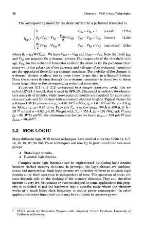
            The corresponding model for the drain current for a p-channel transistor is


        where (3 p - n peW/(T oxL). We have VDS = -Vso  an d VGS - -VsG- Note that both ID P
        and VT P are negative for p-channel devices. The magnitude of the threshold volt-
                  r
        age, VTH> f°  the n-channel transistor is about the same as for the p-channel tran-
        sistor while the polarities of the currents and voltages of an n-channel transistor
        are the opposite of those for a p-channel transistor. The mobility of the charges in
        n-channel devices is about two to three times larger than in p-channel devices.
        Thus, the current flowing through the n-channel transistor is about two to three
        times larger than in the corresponding p-channel transistor.
            Equations (2.1) and (2.2) correspond to a simple transistor model, the so-
                                                 2
        called LEVEL 1 model, that is used in SPICE . The model is suitable for elemen-
        tary analysis of circuits, while more accurate models are required for more accu-
        rate analysis and for devices with submicron channel lengths. Typical values for
                                             2  2               2  2
        a 0.8-^im CMOS process are \i n « 4.62 10~  m /Vs, n p - 1.6 10~  m /Vs, e = 3.9 e 0
        for SiO 2, and e 0 - 8.85 pF/m. Typically T ox is in the range 100 A to 200 A, [1 A =
                                                                           2
           10
        10-  m] and a - 0.02 to 0.05. We get with, T ox « 155 A, ft n « 103 (W/L) uA/V  and
                         2
                                                                           2
        /3 p = 36 (W/L) uA/V . For minimum-size devices we have: f$ nmi n ~ 108 |iA/V  and
                     2
        /Wm-SOuA/V .
        2.3 MOS LOGIC

        Many different logic MOS circuit techniques have evolved since the 1970s [2, 5-7,
        14, 15, 19, 20, 23-251. These techniques can broadly be partitioned into two main
        groups:
            Q Static logic circuits,
            Q Dynamic logic circuits.

            Complex static logic functions can be implemented by placing logic circuits
        between clocked memory elements. In principle, the logic circuits are combina-
        tional and memoryless. Such logic circuits are therefore referred to as static logic
        circuits since their operation is independent of time. The operation of these cir-
        cuits depends only on the clocking of the memory elements. They can therefore
        operate at very low frequencies or even be stopped. In some applications this prop-
        erty is exploited to put the hardware into a standby mode where the circuitry
        works at a much lower clock frequency to reduce power consumption. In other
        applications entire functional units may be shut down to conserve power.


        2
           SPICE stands for Simulation Program with Integrated Circuit Emphasis. University of
           California at Berkeley.

