
Page 113 - Electrical Properties of Materials
P. 113
The field-emission microscope 95
6.7 Field emission
As we have seen in the previous section, the presence of an electric field
increases the emission current because more electrons can escape over the re-
–1
9
duced barrier. If we increase the electric field further, towards 10 Vm , then
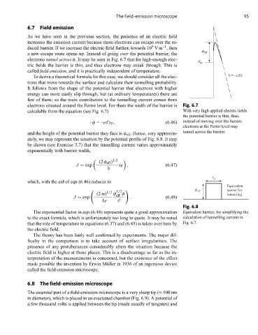
φ eff
a new escape route opens up. Instead of going over the potential barrier, the
electrons tunnel across it. It may be seen in Fig. 6.7 that for high-enough elec-
E F
tric fields the barrier is thin, and thus electrons may sneak through. This is
called field emission, and it is practically independent of temperature.
To derive a theoretical formula for this case, we should consider all the elec- V=–e x
trons that move towards the surface and calculate their tunnelling probability.
It follows from the shape of the potential barrier that electrons with higher
energy can more easily slip through, but (at ordinary temperatures) there are
few of them; so the main contribution to the tunnelling current comes from
electrons situated around the Fermi level. For them the width of the barrier is Fig. 6.7
calculable from the equation (see Fig. 6.7) With very high applied electric fields
the potential barrier is thin, thus,
–φ =–eE x F , (6.46) instead of moving over the barrier,
electrons at the Fermi level may
and the height of the potential barrier they face is φ eff . Hence, very approxim- tunnel across the barrier.
ately, we may represent the situation by the potential profile of Fig. 6.8. It may
be shown (see Exercise 3.7) that the tunnelling current varies approximately
exponentially with barrier width,
1/2
(2 φ eff )
J ∼ exp – x F , (6.47)
x F
which, with the aid of eqn (6.46) reduces to
Equivalent
1/2 1/2 φ eff barrier for
(2 m) φ eff φ tunnelling
J ∼ exp – . (6.48)
e E
Fig. 6.8
The exponential factor in eqn (6.48) represents quite a good approximation Equivalent barrier, for simplifying the
to the exact formula, which is unfortunately too long to quote. It may be noted calculation of tunnelling current in
that the role of temperature in equations (6.37) and (6.45) is taken over here by Fig. 6.7.
the electric field.
The theory has been fairly well confirmed by experiments. The major dif-
ficulty in the comparison is to take account of surface irregularities. The
presence of any protuberances considerably alters the situation because the
electric field is higher at those places. This is a disadvantage as far as the in-
terpretation of the measurements is concerned, but the existence of the effect
made possible the invention by Erwin Müller in 1936 of an ingenious device
called the field-emission microscope.
6.8 The field-emission microscope
The essential part of a field-emission microscope is a very sharp tip (≈ 100 nm
in diameter), which is placed in an evacuated chamber (Fig. 6.9). A potential of
a few thousand volts is applied between the tip (made usually of tungsten) and