
Page 437 - Electrical Properties of Materials
P. 437
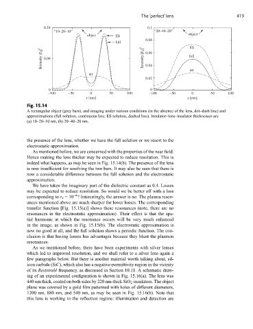
The ‘perfect’ lens                      419

                    0.18                                       0.1
                        “10–20–10”                                “20–40–20”
                                      object      ES                             object
                                                               0.08
                                                  full                           ES
                   Intensity |E 1 | 2  0.09                   Intensity |E 1| 2  0.06  full


                                                               0.04
                                                                                 air
                                       air
                                                               0.02

                      0                                          0
                     –100     –50      0       50      100      –100     –50      0       50      100
                                     x [nm]                                     x [nm]
            Fig. 15.14
            A rectangular object (grey bars), and imaging under various conditions (in the absence of the lens, dot–dash line) and
            approximations (full solution, continuous line; ES solution, dashed line). Insulator–lens–insulator thicknesses are
            (a) 10–20–10 nm, (b) 20–40–20 nm.


            the presence of the lens, whether we have the full solution or we resort to the
            electrostatic approximation.
               As mentioned before, we are concerned with the properties of the near field.
            Hence making the lens thicker may be expected to reduce resolution. This is
            indeed what happens, as may be seen in Fig. 15.14(b). The presence of the lens
            is now insufficient for resolving the two bars. It may also be seen that there is
            now a considerable difference between the full solution and the electrostatic
            approximation.
               We have taken the imaginary part of the dielectric constant as 0.4. Losses
            may be expected to reduce resolution. So would we be better off with a loss
                                –4
            corresponding to ε r =10 ? Interestingly, the answer is no. The plasma reson-
            ances mentioned above are much sharper for lower losses. The corresponding
            transfer function [Fig. 15.15(a)] shows these resonances (note, there are no
            resonances in the electrostatic approximation). Their effect is that the spa-
            tial harmonic at which the resonance occurs will be very much enhanced
            in the image, as shown in Fig. 15.15(b). The electrostatic approximation is
            now no good at all, and the full solution shows a periodic function. The con-
            clusion is that having losses has advantages because they blunt the plasmon
            resonances.
               As we mentioned before, there have been experiments with silver lenses
            which led to improved resolution, and we shall refer to a silver lens again a
            few paragraphs below. But there is another material worth talking about, sil-
            icon carbide (SiC), which also has a negative-permittivity region in the vicinity
            of its Reststrahl frequency, as discussed in Section 10.11. A schematic draw-
            ing of an experimental configuration is shown in Fig. 15.16(a). The lens was
            440 nm thick, coated on both sides by 220 nm-thick SiO 2 insulators. The object
            plane was covered by a gold film patterned with holes of different diameters,
            1200 nm, 880 nm, and 540 nm, as may be seen in Fig. 15.16(b). Note that
            this lens is working in the reflection regime: illumination and detection are