
Page 438 - Electrical Properties of Materials
P. 438
420 Artificial materials or metamaterials
10 2 1.6
full 1.4
ES
1
10 1.2
full
1
|T| 10 0 |E x | 2 0.8
0.6
–1
10 0.4
0.2
ES
10 –2 0
0 5 10 15 20 –200 –100 0 100 200
/k
k x 0 x [nm]
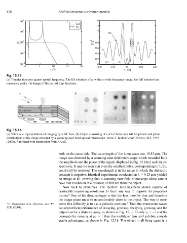
Fig. 15.15
(a) Transfer function against spatial frequency. The ES solution is flat within a wide frequency range; the full solution has
resonance peaks. (b) Image of the pair of step functions.
A B C D
SiO 2 220 nm
SiC Superlens 440 nm
SiO 2 220 nm
60 nm
Au
Fig. 15.16
(a) Schematic representation of imaging by a SiC lens. (b) Object consisting of a set of holes. (c), (d) Amplitude and phase
distributions of the image detected by a scanning near-field optical microscope. From T. Taubner et al., Science 313, 1595
(2006). Reprinted with permission from AAAS.
both on the same side. The wavelength of the input wave was 10.85 μm. The
image was detected by a scanning near-field microscope which recorded both
the amplitude and the phase of the signal, displayed in Fig. 15.16(c) and (d), re-
spectively. It may be seen that even the smallest holes, corresponding to λ/20,
could still be resolved. The wavelength is in the range in which the dielectric
constant is negative. Identical experiments conducted at λ =9.25 μm yielded
no image at all, proving that a scanning near-field microscope alone cannot
have that resolution at a distance of 880 nm from the object.
Now back to principles. The ‘perfect’ lens has been shown capable of
drastically improving resolution. Is there any way to improve its properties
further? One of the disadvantages is that the lens must be thin and therefore
the image plane must be uncomfortably close to the object. The way to over-
∗
∗ E. Shamonina et al., Electron. Lett. 37, come this difficulty is to use a periodic medium. Then the evanescent waves
1243 (2001). can repeat their performance of decaying, growing, decaying, growing, and the
output can be a distance away, as shown in Fig. 15.17. If only ε r = –1 and the
permeability remains at μ r = 1 then the multilayer lens still exhibits consid-
erable advantages, as shown in Fig. 15.18. The object in all three cases is a