
Page 301 - Embedded Microprocessor Systems Real World Design
P. 301
On-Chip Debug
This topic has been mentioned in earlier chapters; it will be addressed in more
detail here.
The addition of on-chip cache memory and high-speed processors complicates
debugging. If instructions are executed from the on-chip cache, there is no
external indication on the processor pins of what is going on. Prefetching causes
problems as well; an instruction may be fetched from memory but never executed.
An incircuit emulator could monitor execution of these instructions, but the high
clock rates of current processors make such an emulator difficult to build.
Another problem with emulators for high-performance processors is packaging.
In the early days of microprocessors, all ICs came in DIP packages that could be
socketed easily. The microprocessor could be removed from the socket and an
emulator installed. Today, many microprocessors come in surface-mount packages
that cannot be socketed. Removing the chip from the board to install an emulator
is not possible, even if there were a way to attach the emulator to the board.
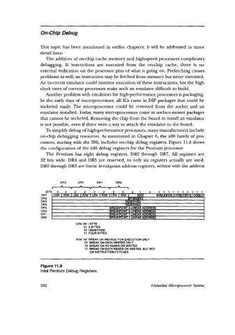
To simplify debug of high-performance processors, many manufacturers include
on-chip debugging resources. As mentioned in Chapter 6, the x86 family of pre
cessors, starting with the 386, includes onchip debug registers. Figure 11.8 shows
the configuration of the x86 debug registers for the Pentium processor.
The Pentium has eight debug registers, DRO through DR7. All registers are
32 bits wide. DR4 and DR5 are reserved, so only six registers actually are used.
DRO through DR3 are linear breakpoint address registers, written with the address
DR3 DR2 DRI DRO
r A I A 7 A I A 3
E1 TS 2 2 2 2 2 2 2 2 2 I 3 1111111111
DR7
DR6
DR5
DR4
DR3
DR2
DR1
OR0
LEN: 00 1 BYTE
01 ZBYTES
10 UNDEFINED
11 FOURBYTES
RIW: 00 BREAK ON INSTRUCTION WECUllON ONLY
01 BREAK ON DATA WRIES ONLY
10 BREAK ON 110 READS OR WRITES
11 BREAD ON DATA READS OR WRITES. BUT NOT
ON INSTRUCTION FETCHES.
Figure 11.8
Intel Pentium Debug Registers.
282 Embedded Micr@rocessar Systems