
Page 70 - Embedded Microprocessor Systems Real World Design
P. 70
MICROPROCESSOR
WPVT BITS
TO OTHER DEUCES
/-
READ STROBE
,
WRITE STROBE
WRITE TIMING
DATA
FROM MICROPROCESSOR
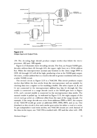
Figure 2.12
Simple Input and Output Ports.
139. The decoding logic should produce output strobes that follow the micro-
processor -RD and -WR signals.
Figure 2.13 illustrates three decoding circuits. The first, an &input NAND gate,
decodes address lines A8 through A15, the upper eight lines on a 16bit address
bus. When the microprocessor accesses any location in the (hex) range FFOO to
FFFF, A8 through A15 will all be high, producing a low at the NAND gate output.
Of course, a wider address bus or a need to decode to greater resolution will require
a wider NAND circuit.
The second circuit in Figure 2.13 is a 74AC138. This circuit produces output
strobes that follow the data strobe from the microprocessor and are suitable for
clocking data into a register or for enabling a buffer. The select inputs (A, B, and
C) are connected to the microprocessor address bus, bits A1 through A2. One
enable is connected to a range decode (such as the NAND gate later in Figure
2.14), and a second enable is connected to the microprocessor data strobe. The
unused enable is pulled up. As indicated in Figure 2.13, the eight outputs of this
circuit each go active at a different offset from the start of the range decode. For
example, if the range decode was active from addresses FFFO to FFF7, the outputs
of the 74AC138 would go active at addresses FFFO, FFF2, FFF4, and so on. One
drawback to this circuit is that each strobe goes active for either a read or a write.
To get independent read/write strobes, two 74AC138 circuits are used. Instead of
the data strobe input, one 74AC138 is enabled with -RD and the other with -WR.
Hardware Design 1 55