
Page 65 - Embedded Microprocessor Systems Real World Design
P. 65
RAS hold time. The minimum time that -RAS must remain low after the
falling edge of -CAS.
RAS/CAS precharge time. The times that -RAS and -CAS must remain high
before the next cycle can start.
Looking at a DRAM data sheet reveals many more timing parameters than those
listed here, but these are the key ones. Note that two access times are listed: RAS
and CAS. The actual access time is determined by the circuit. In a fast circuit, CAS
may enable the output buffer before the logic in the DRAM has decoded the row
address, and the RAS time becomes the actual access time. In a slower circuit, where
the row address will be internally decoded by the time CAS occurs, the access time
will be governed by when CAS falls. To put it another way, data will not be avail-
able from the DRAM any sooner than the RAS time after the falling edge of RAS,
even if the address multiplexing and CAS timing are very fast.
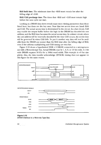
Figure 2.10 shows a hypothetical 256K x 8 DRAM connected to a microproces-
sor with a Motorola-type bus. Actual DRAMS may be 1, 4,8, or 16 bits wide. A 1-bit
wide DRAM requires 16 ICs for a 16-bit word width. This example is x8 for sim-
plicity. Also, the data transfer acknowledge (DTACK) timing does not appear on
this figure for the same reason.
k
MICROPROCESSOR
MULTIPLEXER
AOA17
Ria
-DS nMiffi CAS DATA
RAS
LOGIC
MICROPROCESSOR SIGNALS
AOA17
-DS
DRAM SIGNALS
AOA8
-RAS
-CAS
DATA
TIMING
SEL
Figure 2.10
DRAM Interface to a Motorola-Type Bus.
50 Embedded Microprocessor System