
Page 66 - Embedded Microprocessor Systems Real World Design
P. 66
The address is presented to the DRAM through a multiplexer. At the start of the
cycle (see Figure 2.10), the low-order address bits (A0 through A8) are passed
through to the DRAM and -RAS is pulsed, latching the row address into the DRAM.
After the address hold time is met, the SEL line to the multiplexer is toggled,
causing the high-order address (A9 through A17) to be presented to the DRAM.
After the column address setup time is met, -CAS is pulsed, latching the column
address. Data from the DRAM is available after the CAS access time.
The direction signal (R/W) is passed directly to the DRAM. If the WE pin on
the DRAM is low when -CAS goes low, the DRAM will start a write cycle. If WE goes
low ufte-CAS goes low, the DRAM will do a read cycle, driving read data onto the
data bus, followed by a write cycle. This is called a read dzh Wzte (rmw) cycle. Write
data is latched on the leading edge of -WE or -CAS, whichever is later. Few embed-
ded processors execute rmw cycles. The reason this timing is important is because
you need to avoid bus contention for processors where the write signal may be later
than -CAS. Note, however, that the data is latched and must be stable before -WE
or -CAS, whichever occurs later.
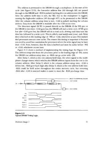
Figure 2.11 shows a method of implementing the timing logic for Figure 2.10.
The address setup time from the processor, prior to the leading edge of -DS, meets
the DRAM row address setup time, so -RAS can go active with -DS.
After Delay 1, which is the row address hold time, the select signal to the multi-
plexer changes states, which switches the DRAM address inputs from the row to the
column address. After Delay 2, which is the column address setup time, -CAS is
driven low. -RAS goes back high after Delay 3, which is the row address hold time.
-RAS could be held active throughout the entire memory cycle, but removing
-RAS after -CAS is asserted makes it easier to meet the -RAS precharge time.
*
SELECT TO ADDRESS MULTIREXER
.CAS TO DRAM
-OS
-DS / -RAS TO DRAM
-RAS 1 /
SELECT /
-CAS /
DELAY 1 -I
DELAY 2
DELAY 3
Figure 2.11
Typical DRAM Timing Logic.
Hardware Design 1 51